Pages

Wednesday, 8 February 2012

20VAC 60 Watt Sunrise Lamp Circuit

20VAC 60 Watt Sunrise Lamp Circuit


This is a circuit for a 120VAC lamp is slowly illuminated over a approximate 20 minute period. The bridge rectifier supplies 120 DC to the MOSFET and 60 watt lamp. A 6.2K, 5 watt resistor and zener diode is used to drop the voltage to 12 volts DC for the circuit power. The bridge rectifier should be rated at 200 volts and 5 amps or more. This is the figure of the circuit;


In operation, a 700 Hz triangle waveform is generated at pin 1 of the LM324 and a slow rising voltage is obtained at pin 8. These two signals are compared at pins 12 and 13 to produce a varying duty cycle rectangular waveform at pin 14, which controls the MOSFET and brightness of the 60 watt lamp. When power is applied, the lamp will start to illuminate within a minute or so, and will slowly brighten to full intensity in about 20 minutes. You can make that longer or shorter with adjustments to the 270K resistor at pin 9. The 2.2 ohm resistor and .015uF cap connected to the lamp serve to supress RFI. The diode at pin 9 and 10K resistor on pin 8 are used to discharge the 3300uF cap when power is removed. Power should be off for a few minutes before re-starting. This circuit is connected directly to the AC line and presents a hazard if any part is touched while connected to the line. Use caution and do not touch any parts while the circuit is connected to the AC line. You may want to use a 9 volt battery connected across the 12 volt zener to check the basic operation. The DC voltage at pins 1,2,3,5,6,7 will all be around 4.3 volts if the circuit is working correctly. If the DC voltages are all correct, you can use a variac to slowly apply the full line voltage and check for proper operation.

Car Interior Light Extender Circuit

Car Interior Light Extender Circuit


This is a circuit for a Courtesy Light Extender for cars. When a door is closed in a car, it extends the ON time, so the passenger can see where he/she is sitting. This is the figure of the circuit;


The light normally goes off immediately when door switch is opened, but the circuit takes over and allows current to flow because the 22u is not charged and the first BC 547 transistor is not turned ON. To illuminate the interior light, this turns on the second BC547 via the 100k and the BD679 is also turned. The 22u gradually charges via the 1M and the first BC547 turns on, robbing the second BC547 of “turn-on” voltage and it starts to turn off the BD679. When the door is opened, the 1N4148 discharges the 22u.

20VAC 60 Watt Sunrise Lamp Circuit

20VAC 60 Watt Sunrise Lamp Circuit


This is a circuit for a 120VAC lamp is slowly illuminated over a approximate 20 minute period. The bridge rectifier supplies 120 DC to the MOSFET and 60 watt lamp. A 6.2K, 5 watt resistor and zener diode is used to drop the voltage to 12 volts DC for the circuit power. The bridge rectifier should be rated at 200 volts and 5 amps or more. This is the figure of the circuit;


In operation, a 700 Hz triangle waveform is generated at pin 1 of the LM324 and a slow rising voltage is obtained at pin 8. These two signals are compared at pins 12 and 13 to produce a varying duty cycle rectangular waveform at pin 14, which controls the MOSFET and brightness of the 60 watt lamp. When power is applied, the lamp will start to illuminate within a minute or so, and will slowly brighten to full intensity in about 20 minutes. You can make that longer or shorter with adjustments to the 270K resistor at pin 9. The 2.2 ohm resistor and .015uF cap connected to the lamp serve to supress RFI. The diode at pin 9 and 10K resistor on pin 8 are used to discharge the 3300uF cap when power is removed. Power should be off for a few minutes before re-starting. This circuit is connected directly to the AC line and presents a hazard if any part is touched while connected to the line. Use caution and do not touch any parts while the circuit is connected to the AC line. You may want to use a 9 volt battery connected across the 12 volt zener to check the basic operation. The DC voltage at pins 1,2,3,5,6,7 will all be around 4.3 volts if the circuit is working correctly. If the DC voltages are all correct, you can use a variac to slowly apply the full line voltage and check for proper operation.

Audio Controlled Incandescent Lamp Light Controller

Audio Controlled Incandescent Lamp Light Controller

This is a design circuit for an audio-controlled lamp circuit. This circuit requires low voltage input such as pre-amplifiers, tone control, or general audio line level output. It’s also possible to feed the input with signal from small power amplifier output, or high power amplifier witk low volume level. The characteristic of lamp dimming (incandescent lamp) will look like coming from proportional controller since the switching rate of the TRIAC would be much higher than the lamp dimming response. This is the figure of the circuit;
 

If the lamp won’t go off after the audio signal back down to zero, then try to adjust the potentiometer. You can use filament transformer (usually used for tube), or you can also use small tv-antenna-booster transformer (20v-220V), or other small transformer below 500mA. Don’t worry if you can’t fine transformer with exact primary-secondary ratio, since the potentiometer is there for fine adjustment, and you can always change the input voltage level of the audio input signal.

DC to AC Inverter Using 555 IC

DC to AC Inverter Using 555 IC

This is a design for AC inverter circuit. This circuit is produces an AC output at line frequency and voltage. The circuit is using 555 IC as main control. This IC is configured a low frequency oscillator, tunable over the frequency range of 50 – 60 Hz by potentiometer R4. This is the figure of the circuit.


The principle work of the circuit is the IC feeds its output that amplified by Q1 and Q2 to input of the transformer T1. A reverse is connected filament transformer with necessary step-up turns ratio. A capacitor C4 and coil L1 filter the input to T1, assuring that it is effectively a sine wave. Adjust the value of T1 to your voltage. Replacement types for Q1 are: TIP41B, TIP41C, NTE196, ECG196, etc. Replacement types for Q2 are: TIP42B, TIP42C, NTE197, ECG197, etc. The input voltage of the circuit is anywhere from +5V to +15Volt DC.

High Voltage DC Generator

High Voltage DC Generator

This is a schematic circuit for voltage generator. This circuit is built by 74C14 IC as generator. This is the figure of the circuit.


This circuit is using power supply 12 VDC. The input to the circuit is then amplified to provide 10000 VDC output. Inside the circuit is there a DC to DC converter. The output of the converter is fed into 10 stage using high voltage multiplier to produce 10,000 VDC.

Wheatston Bridge PWM Signal Conditioner Circuit

Wheatston Bridge PWM Signal Conditioner Circuit


This is a schematic diagram of a Wheatston Bridge PWM Signal Conditioner circuit. This circuit uses the MAX1452 signal conditioner. A ratiometric compensated output for the Wheatstone Bridge is generated by the MAX1452. Then the output of the Wheatston bridge is converted to a PWM output. the PWM-output duty cycle changes accordingly, as the MAX1452 output changes with pressure. the analog-output signal-conditioning ASICs can be used to substitute the MAX1452. This is the figure of the circuit;
 

Frequency counter with pulse-width-measurement option is the instrument that use the circuit. It need an accurate measurement of the PWM output’s pulse width. Beside that, a microcontroller can use the PWM output and the controller’s internal timer to calculate the time interval between high-to-low and low-to-high transitions.  To calculate coefficients required to program the signal-conditioning IC, the measured PWM value can be used. [Circuit schematic source: MAXIM-IC.com]

Pink (Flicker) Noise Generator Circuit

Pink (Flicker) Noise Generator Circuit

Here’s a design circuit for a flicker noise generator, an implementation of flicker noise analog modeling presented in NBS technical note #604, “Efficient Numerical and Analog Modeling of Flicker Noise Processes” by J.A. Barnes and Stephen Jarvis, Jr. With the component values shown the schematic diagram, the circuit will give a 1/f noise slope from below 1Hz to over 4KHz. A TLC2272 op-amp is used for this circuit, but any low noise op-amps will work. This is the figure of the circuit;


The op-amp must be a low noise type because the noise generation come from a high value resistor generating about 50nV noise. Use an op-amp with noise voltage less than 15 nV/root-Hz and noise current less than 0.1 pA/root-Hz, an easy-to-find feature in many low-noise modern op-amp devices. To simplify the construction, the capacitor values is slightly different from the calculated values described in the paper, and a bias circuit is provided to allow the use of polarized electrolytic capacitor. Because the electrolytic capacitor has poor tolerance, it should be chosen carefully for best performance. Compared to circuit utilizing deode zener, reverse-biased transistor, or other noisy devices, this circuit give more predictable and repeatable output level.  If we tap the output of the first op-amp through a 100uF capacitor (like as seen in the second op-amp), a precise 5uV/root-Hz white noise will be there as an excellent signal source for audio noise measurement calibration. At the second op-amp, this white noise is filtered to give a flicker noise (pink noise) frequency spectrum, since the pink noise is a subset of white noise in the frequency domain. [Circuit diagram source: techlib.com]

Active Crossover Circuit: Split The Audio Signal Before Amplification

Active Crossover Circuit: Split The Audio Signal Before Amplification


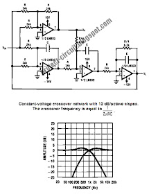
You might be familiar with passive crossover network installed inside your speaker box, consist of inductors and capacitors. The problem with passive crossover network is that they dissipate the audio power, so it’s not environmentally friendly, contributing a little disaster of global warming. Moreover, the capacitor and the inductor in the passive crossover network contribute the distortion of the signal since it must drive a low impedance load (the loud speaker). The best way to get high quality audio is to separate the high and low frequencies before feeding the signal to the amplifier. The drawback is that you need two amplifiers, to amplify the low and high audio signal separately. This is the figure of the circuit;


The circuit use a constant voltage method, means that the output of high and low frequency is summed up, and then fed back to be compared with the input to make sure this sum is equal to the input signal. This method is ensures that the total response is flat, if we summed back the separated high and low frequency output. You have to use 1% tolerance for the resistors to give a precise response. According to the formula, the capacitor C should be 6.6nF to give 1kHz crossover frequency, but a 6.8nF can be used because it widely available, and the crossover frequency will be shifted to about 975Hz.

[Circuit schematic diagram source: National Semiconductor Application Notes]

Tone Control Circuits Using CA3140

Tone Control Circuits Using CA3140

This is a circuit for tone control in the amplifier. High slew rate, wide bandwidth, high output voltage capability and high input impedance are all characteristics required of tone control amplifiers. This circuit is built by CA3140 IC. Ca3140 is a op amp for audio signal. This is the figure of the circuit.


The Baxandall tone control circuit which is provides unity gain at mid band and uses standard linear potentiometers. The high input impedance of the CA3140 makes possible the use of low cost, low-value, small size capacitors, as well as reduced load of the driving stage. Bass treble boost and cut are 15 dB at 100 Hz and 10 KHz, respectively. Full peak-to-peak output is available up to at least 20 KHz due to the high slew rate of the CA3140. The amplifier gain is 3dB down from its “flat” position at 70 KHz.

[Project Schematic source: Intersil Corporation]

Active Crossover Circuit: Split The Audio Signal Before Amplification

Active Crossover Circuit: Split The Audio Signal Before Amplification


You might be familiar with passive crossover network installed inside your speaker box, consist of inductors and capacitors. The problem with passive crossover network is that they dissipate the audio power, so it’s not environmentally friendly, contributing a little disaster of global warming. Moreover, the capacitor and the inductor in the passive crossover network contribute the distortion of the signal since it must drive a low impedance load (the loud speaker). The best way to get high quality audio is to separate the high and low frequencies before feeding the signal to the amplifier. The drawback is that you need two amplifiers, to amplify the low and high audio signal separately. This is the figure of the circuit;


The circuit use a constant voltage method, means that the output of high and low frequency is summed up, and then fed back to be compared with the input to make sure this sum is equal to the input signal. This method is ensures that the total response is flat, if we summed back the separated high and low frequency output. You have to use 1% tolerance for the resistors to give a precise response. According to the formula, the capacitor C should be 6.6nF to give 1kHz crossover frequency, but a 6.8nF can be used because it widely available, and the crossover frequency will be shifted to about 975Hz.

[Circuit schematic diagram source: National Semiconductor Application Notes]

Multiple Output DC-DC Converters and Doubles as High-Voltage DC-DC Controllers

Multiple Output DC-DC Converters and Doubles as High-Voltage DC-DC Controllers

This is a design circuit for converter that is ideal for use as a secondary-side post regulator in the design of multiple output AC-DC or DC-DC power supplies or as a DC-DC controller for use in point-of-load (POL) regulators. This circuit is work with based on LM5115. This is the figure of the circuit;


This IC in the circuit has features provide multiple outputs from main DC-DC or AC-DC converter. This IC has operates directly from secondary-side phase signal or DC input. The LM5115 is leading-edge modulation for SSPR from current-mode primary controller. This IC has integrated gate drivers with 2.5A peak output current. Up to 1 MHz switching frequency reduces component footprint and profile. [Circuit source: MAXIM Application Notes]

6V - 12V Converter Circuit

6V - 12V Converter Circuit

This circuit is an inverter actually. This circuit is not converter, but it is say as converter cause convert voltage from low to high. This inverter circuit can provide up to 800mA of 12V power from a 6V supply. For example, you could run 12V car accessories in a 6V of the car. The circuit is simple, about 75% efficient and quite useful. This is the figure of the circuit.


This circuit is work based on transistor. L1 is a custom inductor wound with about 80 turns of 0.5mm magnet wire around a toroidal core with a 40mm outside diameter. Different values of D3 can be used to get different output voltages from about 0.6V to around 30V. Note that at higher voltages the circuit might not perform as well and may not produce as much current. You may also need to use a larger C3 for higher voltages and/or higher currents. You can use a larger value for C3 to provide better filtering. The circuit will require about 2A from the 6V supply to provide the full 800mA at 12V.

Part:
R1, R4 2.2K 1/4W Resistor
R2, R3 4.7K 1/4W Resistor
R5 1K 1/4W Resistor
R6 1.5K 1/4W Resistor
R7 33K 1/4W Resistor
R8 10K 1/4W Resistor
C1,C2 0.1uF Ceramic Disc Capacitor
C3 470uF 25V Electrolytic Capcitor
D1 1N914 Diode
D2 1N4004 Diode
D3 12V 400mW Zener Diode
Q1, Q2, Q4 BC547 NPN Transistor
Q3 BD679 NPN Transistor
L1 See Notes MISC1Heatsink for Q3, Binding Posts (for Input / Output), Wire, Board

Versatile Boost Converter with TPS6108x

Versatile Boost Converter with TPS6108x

This is design circuit for converter. There are two types of highly integrated boost converters, the TPS61081 and TPS61080. Both of them require low input voltage of 2.5V and the output is adjustable up to 27 V. The TPS61080’s current limit rating of the integrated power switches is 0.5 A and 1.3 A for TPS61081. This is the figure of the circuit;


It is useful for industrial application such as a 12- or 24-V industrial power rail from a 3.3- or 5-V bus. It also can be used to boost the 3.6-V Li-ion battery voltage used in most portable applications. Besides that, it can be used for higher voltages required applications such as OLED displays, powering thin film-transistor (TFT) LCDs, camera flashlights or WLED backlights.

For light-load efficiency, we can configure the switching frequency about 600kHz and 1.2 MHz for smaller external components . An extremely small boost converter is enabled by the 3 × 3-mm QFN package for a wide variety of applications because it has, fast PWM switching and internal power switches, and integrated feedback compensation. [Source: Texas Instruments Application Note]

Boost Converter Circuit for Digital Camera Motor Using LM2623

Boost Converter Circuit for Digital Camera Motor Using LM2623

This is a design circuit for converter that using for a very practical LM2623A ratio adaptive circuit to drive a digital camera motor. It produces 5 volts from input voltages ranging between 1.8 and 4.5 volts. This is the figure of the circuit;


The duty cycle is not shown, but it varies from about 86% at 1.8 volts in to 71% at 4.5 volts in. Maintaining the 86% duty cycle at 4.5 volts would reduce the efficiency and increase the ripple. Maintaining the 70% duty cycle at 1.8 volts would significantly reduce the output capability. Several camera manufacturers are already requiring 1.8 to 4.5 volt operation from all the power supplies. The 1.8 to 4.5 voltage standard allows a manufacturer to build his product and let the user select disposable Alkalines, Ni-MH or Li-Ion at the point of purchase.

[Schematic circuit source: National Semiconductor Notes]

Synchronous Buck Converter Circuit

Synchronous Buck Converter Circuit

This is a design for synchronous buck converters. A synchronous buck converter consists of a high side and a low-side MOSFET, which is placed in place of the conventional buck converter catch diode to provide a lower loss path for the load current. Shoot-through leads to current spikes at the switching instants and manifests itself as a decrease in the efficiency of the converter. A current probe cannot be used to measure it because the inductance of the probe significantly affects the circuit operation. An alternative way to detect shoot through is by looking for spikes on the gate source voltages of the two FETs. (The gate-source voltage of the top MOSFET can be monitored differentially). This is the figure of the circuit;


One approach is to employ a controller IC with a “fixed dead-time,” which ensures that there is a delay after the top MOSFET is turned-off before the lower MOSFET is turned on. This approach is simple, but has to be implemented carefully. If the dead time is too short, shoot-through may not be averted. If it is too long, the conduction losses increase because during the dead time the body diode of the bottom FET is on. Because of the conduction of this body diode during the dead-time, the efficiency of the system when using this technique depends somewhat on the bottom MOSFET’s body diode characteristics.

Stereo Audio Coder-Decoder Circuit

Stereo Audio Coder-Decoder Circuit


This is a design circuit for audio coder and decoder. This audio coder-decoder is suitable for home and portable applications like MD, CD and MP3 players. This circuit uses UDA1380 for main components. This is the figure of the circuit;


The UDA1380 is a stereo audio coder-decoder, available in TSSOP32 (UDA1380TT) and HVQFN32 (UDA1380HN) packages. All functions and features are identical for both package versions. The term ‘UDA1380’ in this document refers to both UDA1380TT and UDA1380HN, unless particularly specified. The front-end of the UDA1380 is equipped with a stereo line input, which has a PGA control, and a mono microphone input with an LNA and a VGA. The digital decimation filter is equipped with an AGC which can be used in case of voice-recording.

The DAC part is equipped with a stereo line output and a headphone driver output. The headphone driver is capable of driving a 16 W load. The headphone driver is also capable of driving a headphone without the need for external DC decoupling capacitors, since the headphone can be connected to a pin VREF (HP) on the chip.

[Circuit schematic diagram source: Phillips Semiconductor Notes]

Voltage to Pulse Duration Converter Circuit

Voltage to Pulse Duration Converter Circuit


This is a design circuit for voltage to pulse duration converter. This circuit is control using op amp 741. This is the figure of the circuit;


This circuit is used to convert voltage into pulse duration by combining a timer IC and an OP Amp. This circuit can obtain accuracy up to better than 1%. The output signal is independent of the input voltage and still retain the original frequency.

[Circuit source: Philips Semiconductor Notes]

YPBPR to RGB Video Converter Circuit Using LT6552

YPBPR to RGB Video Converter Circuit Using LT6552

This is a design circuit for LT6552 amplifiers connected to convert component video (YPBPR) to RGB. This is the figure of the circuit;


The LT6552 is a video difference amplifier optimized for low voltage single supply operation. The LT6552 features 75MHz – 3dB bandwidth, 600V/µs slew rate, and ±70mA output current making it ideal for driving cables directly. This circuit maps the sync on Y to all three outputs, so if a separate sync connection is needed by the destination device.

Anti-Log Converter Circuit

Anti-Log Converter Circuit

Anti-log or exponential generation is simply a matter of rearranging the logarithmic circuitry. The circuitry of the log converted to generate an exponential output from a linear input. This is the figure of the circuit;


The emitter of Q2 in proportion to the input voltage is driven by amplifier A1 in conjunction with transistor Q1. The collector current of Q2 varies exponentially with the emitter-base voltage. [Circuit diagram source: National Semiconductor Application Note]

Op Amp Digital to Analog Converter Circuit

Op Amp Digital to Analog Converter Circuit

This is a design of the simple 4-bit digital-to-analog converter.  It is actually just a variant of a simple op amp summer circuit, i.e., an operational amplifier configured to output a voltage that is proportional to the sum of the input voltages. Here’s the figure of the circuit;


In this circuit, the inputs are binary weighted with respect to each other, with the binary weighting of the inputs achieved by the R-2R ladder resistor network at the non-inverting input of the op-amp. As its name implies, the R-2R network consists of resistors with only two values, R and 2R (10K and 20K, respectively, in the circuit shown).  The input SN to bit N is '1' if it is connected to a voltage VR and '0' if it is grounded. The number of bits of this DAC may be increased by connecting more switches with corresponding R/2R resistors.

Low Power Universal Demultiplexer/Decoder

Low Power Universal Demultiplexer/Decoder

This is a circuit for universal decoder that has functions as either a dual 1-of-4 decoder or as a single 1-of-8 decoder, depending on the signal applied to the Mode Control (M) input. Here’s the figure of the test circuit;


In the dual mode, each half has a pair of active-LOW Enable (E) inputs. Pin assignments for the E inputs are such that in the 1-of-8 mode they can easily be tied together in pairs to provide two active-LOW enables (E1a to E1b, E2a to E2b). Signals applied to auxiliary inputs Ha, Hb and Hc determine whether the outputs are active HIGH or active LOW. In the dual 1-of-4 mode the Address inputs are A0a, A1a and A0b, A1b with A2a unused (i.e., left open, tied to VEE or with LOW signal applied). In the 1-of-8 mode, the Address inputs are A0a, A1a, A2a with A0b and A1b LOW or open. All inputs have 50 kX pull down resistors. [Circuit diagram source: National Semiconductor Application Notes]

5VDC to 12VDC LT1070 Boost Converter Circuit

5VDC to 12VDC LT1070 Boost Converter Circuit

Here’s a design circuit for 5VDC to 12VDC boost converter circuit built based LT1070. This is the figure of the circuit;


The LT®1070/LT1071 are monolithic high power switching regulators. They can be operated in all standard switching configurations including buck, boost, fly back, forward, inverting and “Cuk”. A high current, high efficiency switch is included on the die along with all oscillator, control and protection circuitry.

Low Impedance Loads Using LT1210 IC

Low Impedance Loads Using LT1210 IC

This is a circuit for impedance load of voltage. This circuit is work using transformer coupling that is frequently used to step up transmission line signals. This circuit is based on LT1210 IC. This IC is fast and capable of delivering high levels of current. They can be readily compensated for reactive loads and are fully protected against thermal and short-circuit faults. This circuit is simple design. This is the figure of the circuit.


The operation of this circuit is begun from a transformer-coupled application for ADSL in which an LT1210 drives a 100W twisted pair. The 1:3 transformer turns ratio allows just over 1W to reach the load at full output. Resistor RT acts as a primary side back termination and also prevents large DC currents from flowing in the coil. The overall frequency response is flat to within 1dB from 500Hz to 2MHz. Distortion products at 1MHz are below – 70dBc at a total output power of 0.56W (load plus termination), rising to –56dBc at 2.25W. If RT is removed, the amplifier will see a load of about 11W and the maximum output power will increase to 5W. A DC blocking capacitor should be used in this case. [Schematic source: Linear Technology Corporation, Inc].

3 Band Equalizer Circuit

3 Band Equalizer Circuit

This is a circuit for a tone control using 3 band equalizers. This circuit is based on single chip op amps LF351. This circuit having three ranges, bass, middle and treble controls. This is the figure of the circuit;


With a single chip op amps LF351, it is easy to make equalizer offers three ranges, low frequency, mid frequency, and high. With component values shown there is approximately +/-20dB of boost or cut at frequencies of 50Hz, 1kHz and 10kHz. Supply voltage may be anything from 6 to 30 Volts. Maximum boost 20dB is only realized with maximum supply voltage of 18 Volt.

Audio Graphic Equalizer Circuit

Audio Graphic Equalizer Circuit

This is a project circuit for audio equalizer. This circuit is control by single chip op amps. This is the figure of the circuit;


A gyrator is a circuit using active devices and transistors to simulate an inductor. In this case the gyrator is the transistor acting with R1, R3 and C2. It could just as easily be a unity gain op-amp (which gives superior performance). The circuit includes three formulae: one which gives f, the centre frequency of the band. The second shows how the Q is related to the capacitor ratio. The third shows the impedance presented by the circuit. Note that this includes 3 terms, the first purely resistive, the second is the capacitive contribution from C1 and the third is an inductive term from the gyrator.

Voltage Cut Off Circuit Using Time Delay

Voltage Cut Off Circuit Using Time Delay

This is a design for protection voltage. This circuit is called as high and low voltage cut off. The circuit is using time delay for cut off the voltage. This is a low cost and reliable circuit for protecting such equipments from damages. This is the figure of the circuit.


Whenever the power line is switched on it gets connected to the appliance only after a delay of a fixed time. If there is hi/low fluctuations beyond sets limits the appliance get disconnected. The system tries to connect the power back after the specific time delay, the delay being counted from the time of disconnection. If the power down time (time for which the voltage is beyond limits) is less than the delay time, the power resumes after the delay: If it is equal or more, then the power resumes directly. This circuit is using op-amp 741 and 555 IC for control the operation.

The complete circuit is consisting of various stages. They are: - Dual rail power supply, Reference voltage source, Voltage comparators for hi/low cut offs, Time delay stage and Relay driver stage. Under normal operating conditions i.e. when the input voltage is between maximum and minimum limit the output from the both the comparators are low. The transistor Q1 is OFF and the relay is in de-energized (pole connected to N/C pin) state and the output is obtained. When the input voltage is below or above the limits set by the pre-sets R8 or R9, the output of the Op-Amps goes either low or high and diodes D1 or D2 would be forward biased depending on the situation. Transistor Q1 switches ON and the flow of current from collector to emitter energizes the relay and the output is cutoff.

The Butterworth Second Order High Pass Filter Circuit

The Butterworth Second Order High Pass Filter Circuit

This is a circuit for high pass filter. This circuit is similar to low-pass filter circuit, but the position for resistors and capacitor are interchanged. This circuit is based on op-amp for the operation. LM833 IC is the op-amp that is used in the circuit. This is the figure of the circuit.


Similar with low pass design guide, the resistor and capacitor should be chosen according to the formula, and the resistor value should be:
· Much higher than equivalent leakage resistance of the capacitor.
· Much higher than the operational-amplifier’s (op-amp’s) input impedance.
· Doesn’t draw excessive current-violating the maximum allowed op-amp’s output current.

In general, for higher capacitor value, it is leakage current would be higher and you must use lower resistors to compensate the capacitor’s current leakage. [Schematic source: National Semiconductor's LM833 Application Notes]

The Video Limiter Circuit

The Video Limiter Circuit

This circuit is use to avoid exceeding luminance reference level standard or to avoid exceeding the input range of digitizer (ADC), video signal is often needed to be limited. The simple way to do this is by hard limiting the signal in the positive direction (white peak clipping), but this method completely destroy all information contained in the clipped region. This circuit is based on LT1228 IC’s. This circuit is called as video limiter. This is the figure of the circuit.


The better way to limit the signal is while preserving all information contained in the signal is by soft limiting the signal, where the signal will be compressed at the above threshold region. The LT1228 is used here in a slightly unusual, closed-loop configuration. The gain of the closed-loop is set by the feedback and gain resistors (RF and RG) and the open-loop gain by the trans-conductance of the first stage times the gain of the CFA. The level at which the limiting action begins is adjusted by varying the set -current into pin 5 of the trans-conductance amplifier.
[Schematic diagram source: Linear Technology Application Notes]

Low Pass Filter Circuit for Subwoofer

Low Pass Filter Circuit for Subwoofer

This is a design schematic for filter the subwoofer that is purpose for distinguishes these frequencies, in order to him we lead to the corresponding amplifier. The acoustic filters are met in various points in the sound systems. In the circuit is built by op amps. This is the figure of the circuit.


The acoustic spectrum is extended by very low frequencies 20Iz and reaches as the 20000Iz in high frequencies. In the low frequencies is degraded the sense of direction. This reason is leads to the utilization speaker for the attribution of very low frequencies. The application is a simple filter of region that limits the acoustic region (20-20000Hz) in the region 20-100Hz. This circuit is constitutes mixed, amplifier with variable aid and a variable filter.

Parts:

R1 = 39 Kohm R2 = 39 Kohm
R3 = 47 Kohm R4 = 10 Ohm
R5 = 22 Kohm R6 = 4,7 Kohm
R7 = 22 Kohm R8 = 4,7 Kohm
R9 = 10 Ohm R10 = 220 Ohm
C1 = 39 pF C2 = 0.1 uF
C3 = 0.1 uF C4 = 0.2 uF
C5 = 0.4 uF C6 = 0.1 uF
C7 = 0.1 uF IC1 = TL064

Positive Feedback Circuit Using LM111

Positive Feedback Circuit Using LM111

This is the circuit that is due to the high gain and wide bandwidth of comparators. This circuit is built by op amps LM111. This is the figure of the circuit.


The trim pins (pins 5 and 6) act as unwanted auxiliary inputs. If these pins are not connected to a trim-pot, they should be shorted together. If they are connected to a trim-pot, a 0.01 mF capacitor C1 between pins 5 and 6 will minimize the susceptibility to AC coupling. A smaller capacitor is used if pin 5 is used for positive feedback. When the signal source is applied through a resistive network, RS, it is usually advantageous to choose an RSÊ of substantially the same value, both for DC and for dynamic (AC) considerations. Carbon, tin-oxide, and metal-film resistors have all been used successfully in comparator input circuitry. Inductive wire wound resistors are not suitable. [Circuit source: National Semiconductor, Inc]

Multiple Feedback Filter Using Differential Low Pass Filter Circuit

Multiple Feedback Filter Using Differential Low Pass Filter Circuit

This is a circuit for low pass filter that can be used for multiple feedback filter. The filter is a two pole filter topology used to implement an electronic filter by adding two poles to the transfer function. This is available in a low pass, high pass, band pass, and notch versions, although the band pass and notch versions are not recommended because of the low resistor values. Some Feedback filters are useful for distribution, analysis and other tasks such as the Sound to light converter or a fully functional Vocoder. This is the figure of the circuit.


The circuit above shows an example of Multiple Feedback Filter with Differential Low Pass Filter Circuit Schematic Diagram. The table below contains details of the transfer functions (Bessel, Butterworth, and Chebyshev 3 dB).
Bessel
For = 1 / (2pRC)
R1 = R2 = 0.625R
R3 = 0.36R
C1 = C
C2 = 2.67C
Butterworth
For = 1 / (2pRC)
R1 = R2 = 0.65R
R3 = 0.375R
C1 = C
C2 = 4C
Chebyshev 3 dB
For = 1 / (2pRC)
R1 = 0.644R
R2 = 0.456R
R3 = 0.267R
C1 = 12C
C2 = C

Low Pass Filter Circuit with Enhanced Step Response

Low Pass Filter Circuit with Enhanced Step Response

Effect on the system’s time-domain response is a common problem when designing low-pass filters. The system may fail to recognize significant changes in time because pushing the cut-off frequency lower slows the step response. For solving the problem, this is the figure of the circuit.


On this circuit diagram, lower cut-off frequency is allowed without sacrificing the step-response time. The delta (difference) between the filter’s input and output is monitored by window comparator. The filter increases its slew rate by increasing its cut-off frequency an order of magnitude when the delta exceeds 50mV. Low-pass-filtered by R4 and C3 is the original signal which is producing a cut-off frequency (312Hz) that reduces sensitivity to momentary glitches. The window-comparator input is drove by the filtered input. Comparator U2A or U2B will assert its output low if the input is outside the 50mV window. The low output drives Q5 into cutoff, causing its collector to presume a high impedance.

The filter’s cutoff frequency increases by ten times because the Q5 collector no longer grounds capacitor C2. The cutoff frequency throttles back to its quiescent state. When the system output changes to within 50mV of the system input. This circuit diagram is configured for very low cutoff frequency, but changing C1 and C2 can rescale the configuration to higher frequency, where the oscillation frequency fOSC (in kHz) is 30 x 103/COSC (in pF) and the cutoff frequency is fOSC/100. For different window values in which the delta equals the resistance multiplied by 115µA, we can modify R2 and R3. The type of comparator must be an open-drain type.

[Source: maxim-ic.com]

High Efficiency Filter Circuit 3W Switching Audio Amplifier

High Efficiency Filter Circuit 3W Switching Audio Amplifier


This is a design circuit for filter circuit for amplifier. This circuit is a simple design circuit that is based on LM4670. This is the figure of the circuit;


The LM4670 is designed to meet the demands of mobile phones and other portable communication devices. Operating on a single 5V supply, it is capable of driving a 4 speaker load at a continuous average output of 2.3W with less than 1% THD+N. Its flexible power supply requirements allow operation from 2.4V to 5.5V. The LM4670 has high efficiency with speaker loads compared to a typical Class AB amplifier. With a 3.6V supply driving an 8 speaker, the IC's efficiency for a 100mW power level is 77%, reaching 88% at 600mW output power. [Schematic circuit source: National Semiconductor Notes].

Low Pass Filter Subwoofer Circuit Using TL062

Low Pass Filter Subwoofer Circuit Using TL062


This is a circuit for subwoofer circuit. This circuit is simple design that is based on TL IC. This is the figure of the circuit;

In the form it appears the theoretical circuit of filter. In first glance we see three different circuits that are mainly manufactured round two operational amplifiers. This circuits constitute mixed, amplifier with variable aid and a variable filter. The manufacture end needs a circuit of catering with operational tendency of catering equal with ±12. the operational amplifiers that constitute the active elements for this circuits of are double operational type as the TL082 and NE5532. The operational these amplifiers belong in a family provided with transistor of effect of field IFET in their entries. Each member of family allocates in their circuit bipolar transistor and effect of field. This circuits can function in his high tendency, because that they use transistor of high tendency. Also they have high honor of rhythm of elevation (slew rate), low current of polarization for the entries and are influenced little by the temperature. The operational these amplifiers have breadth of area unity gain bandwidth 3MHz. A other important element for their choice is the big reject of noise, when this exists in the line of catering.

TL084 Audio Compressor (AGC) Circuit

TL084 Audio Compressor (AGC) Circuit


Compressor or AGC (automatic gain control) is used to manipulate the average amplitude of audio signal, to produce relatively constant volume of signal from high dynamic signal source. The 2N3819 JFET (which is used as a voltage controlled resistor) is the key component. Control voltage which is derived by full-wave rectification followed by a peak detector is provided by the output of the circuit. The full wave rectifier is called a precision absolute value circuit can be found in Tobey, Graeme and Huelsman’s : “Operational Amplifier” (1971)- page 249. Several matched resistor is required by the circuit for correct operation and alternative versions of this sub-circuit, which require fewer matched resistors and overall fewer components, could be advantageously substituted. This is the figure of the design circuit;


The product of R4 and the 4.7 uF capacitor is determine the attack time. It’s becomes reverse biased when the input signal drops D1 and the decay time constant is determined by R5. (Since the original publication date I have discovered that the term ‘release’ is used rather than ‘decay’ in the case of compressors.) Both time constants are something of a compromise, the decay must be fast enough to allow low amplitude signals shortly following high amplitude ones to be given sufficient gain and the attack must be fast if the start of high amplitude signals are not to be overloaded until the gain reduces. After long periods of silence or low amplitude inputs, the problem occurs. The next high amplitude signal will get the ‘full gain treatment’ and so will initially overload the circuit and some distortion will be result. Reduce R4 to zero resulting in minimal attack time (determined by the maximum output current of IC3) is the best that could be done under these circumstance. The circuit is by no means ‘hi-fi’ but will be useful for AGC in tape-recording, radio and signal processing where a signal’s large dynamic range needs to be reduced. The original circuit uses 741 IC for the op-amps and OA81 for the diodes (D1,D2,D3).

Subwoofer Filter Circuit

Subwoofer Filter Circuit

This is a circuit of subwoofer active filter circuit is a 24 dB octave filter with a Bessel character and cutoff frequency of 200 Hz. So, if you are interested in experimenting with audio circuits in subwoofer range, this circuit is for you. This is the figure of the circuit;


In subwoofer range, all audio frequencies below 200 Hz can be fed to a single speaker box since the human directional perception of sound diminishes at this frequency range. The normal stereo signals above 200 Hz can be fed to two satellite speaker boxes. How does the subwoofer filter works: A1 and A2 buffer the signals coming from right and left channels. Op amp combinations A2/A4 and A9/A10 function as the high pass filters. The outputs are then connected to the final amplifiers of the battelite boxes. Signals from both channels are fed to A5. Op amps A6/A7 function as the low pass filter, A8 as the output amplifier for the subwoofer signal.

The signal level can be balanced between the subwoofer and the satellite lines. The power needed for this filter circuit must ne a symmetrical power supply. The op amps can have either JFET or bipolar inputs.

Wide Band Two Pole High Pass Filter Circuit

Wide Band Two Pole High Pass Filter Circuit

This is a circuit for high input impedance of the LH0033 and LH0063 are suitable for active filter applications. A basic two pole, high pass filter is diagrammed in circuit using the LH0033. Here’s the figure of the circuit;


This circuit provides a 10 MHz cutoff frequency. One consideration of the filter is its apparent gain change due to the finite output impedance of the amplifier, which affects the overall gain and the damping factor of the filter stage. Resistor R3 ensures that the input capacitance of the amplifier does not interact with the filter response at the frequency of interest. An equivalent low pass filter is similarly obtained by capacitance and resistance transformation. [Circuit diagram source: National Semiconductor Application]

Single Chip Theremin Circuit

Single Chip Theremin Circuit

This is a design circuit for a single chip Theremin circuit.  Theremin is an electronic music instrument which sense hand movement to control the tones/frequency.  This Theremin circuit uses two separate Colpitts LC oscillators to produce a beat frequency. The frequencies of two Colpitts LC oscillators are mixed and then rectified. This rectification demodulate the mixed signal to get the beat frequency which is in audible range. This is the figure of the circuit;


This beat frequency or difference is the real Theremin’s output. The oscillator is operated at high frequency (inaudible) to get wide audible frequency range of beat frequency when two oscillator output is mixed.  This circuit uses a 4011 quad gate to construct the high frequency oscillator operating at 250kHz. The metal probe that is used to sense your  hand produces only small frequency shift in term of percentage of original frequency, that’s why we need to derive the beat frequency to get wide audible frequency range as the result of  high frequency shifting. The IC2, an LM741 is used to amplify the mixed signal before rectification. The D1 will rectify the mixed signal to detect the audio (the beat frequency).  This audio signal is then filtered by an adjustable band pass filter IC3. The further audio amplification before power amplifier IC5  is done by IC4. The metal toilet-tank float  is used for the hand probe since is has better sensitivity than a simple wire antenna, but any conductive material will work. [Circuit diagram source: seekic.com]

15 Channels Cascaded MAX455 Video Mux

15 Channels Cascaded MAX455 Video Mux

Here’s a circuit for showing two MAX455s IC chip are cascaded to build a 1 of 15 video Multiplexer. This is the figure of the circuit;


This cascading is done by connecting the output of one MAX455 MUX to one input of a second MAX455 MUX. The output of the first MUX should be terminated to ground using a 75R resistor, to preserve bandwidth although the two devices are usually close to one another

DC to AC Inverter

DC to AC Inverter

This is design circuit for inverter. This circuit is convert DC to AC voltage. This circuit is work based on 555 IC. This is the figure of the circuit.


The work of the circuit is producing high voltage output and frequency. The function of the IC is as low frequency oscillator and tuned for frequency 50 to 60 Hz. For adjustment is using potentiometer R4. The IC feeds the output to amplified using TIP to the input by transformer. The capacitor and the coil is used as assuring the effectively sine wave.

Light Dependent Resistor Circuit

Light Dependent Resistor Circuit


The Light Dependent Resistor and a trimpot form a voltage divider which is used to apply bias to a transistor. As the LDR changes resistance the change in potential is detected by the circuit and the relay is activated. The PCB-mounted switch just interchanges the trimpot & the LDR as far as the detection circuit is concerned. So a dark activated switch becomes a light activated switch or vice versa. This is the figure of the circuit;


An LED with current limiting resistor is in parallel to the relay to give a visual indication of when the relay is turned on. The relay (Use a 5A/250VAC) can be connected to a light bulb and power supply which will light up when the environment is bright or vice versa. This circuit is satisfactory if the changes in light level to be detected are large and the transition is quick - for example, a person walking past a doorway. An inherent problem of the circuit is chattering of the relay for slowly changing light levels just at the transition point between turning on/odd and vice versa. This leads to the relay chattering as it rapidly turns on/off. This problem can be overcome in by having a hysteresis circuit using an op-amp or a Schmidt Trigger.

Colpitts Crystal Oscillator Circuit

Colpitts Crystal Oscillator Circuit

This is a design schematic of a Crystal Colpitts oscillator can be implemented using a transistor and a parallel mode crystal. This is the figure of the circuit.


In this circuit, the crystal is use as an inductance. A large value capacitive divider is used between gate, source, and ground, and a small series capacitor is placed in the crystal circuit. You should choose the components values so that C2+C3 to C1 ratio has the highest possible value. The ratio of 5 to 10 to 1 is usually used. The schematic shows the typical values. This circuit introduce is a little loading on the crystal. The relatively high value is of C2 and C3 “swamp out” variations and drift caused by variations in device characteristics. Frequency can be fine tuned with C1. A clean enough sine wave appears at the emitter of the transistor.

Low Distortion Sine Wave Oscillator with op-amp

Low Distortion Sine Wave Oscillator

One approach to generating sine waves is to filter a square wave. This leaves only the sine wave fundamental as the output. Since a square wave is easily amplitude stabilized by clipping, the sine wave output is also amplitude stabilized. For the solution of the problem, you can look at the figure below.


A lower distortion oscillator is needed. It can be used. Instead of driving the tuned circuit with a square wave, a symmetrically clipped sine wave is used. The clipped sine wave, of course, has less distortion than a square wave and yields a low distortion output when filtered. This circuit is not as tolerant of component values as tune sine wave oscillator. To insure oscillation, it is necessary that sufficient signal is applied to the zener for clipping to occur.

Clipping about 20% of the sine wave is usually a good value. The level of clipping must be high enough to insure oscillation over the entire tuning range. If the clipping is too small, it is possible for the circuit to cease oscillation due to tuning, component aging, or temperature changes. Higher clipping levels increase distortion. [Schematic’s diagram source: National Semiconductor. Inc]

Phase Shift Oscillator Circuit

Phase Shift Oscillator Circuit

This is a design circuit of a simple inexpensive amplitude stabilized phase shift sine wave oscillator which requires one IC package, three transistors and runs off a single supply. This circuit is combination with the RC network comprises a phase shift configuration and oscillates at about 12 kHz. The remaining circuitry provides amplitude stability. Here’s the schematic figure of the circuit.


The high impedance output at Q2's collector is fed to the input of the LM386 via the 10 μF-1M series network. This circuit is using op amp LM386 causes it has fixed gain of 20. The 1M resistor in combination with the internal 50 kΩ unit in the LM386 divides Q2's output by 20. The positive peaks at the amplifier output are rectified and stored in the 5 μF capacitor. This potential is fed to the base of Q3. Q3's collector current will vary with the difference between its base and emitter voltages. Since the emitter voltage is fixed by the LM313 1.2V reference, Q3 performs a comparison function and its collector current modulates Q1's base voltage. Q1, an emitter follower, provides servo controlled drive to the Q2 oscillator.a

Wien Bridge Oscillator Circuit

Wien Bridge Oscillator Circuit

This is a circuit that is known as wien bridge oscillator circuit. The circuit has positive and negative feedback loop. This circuit is work with control by op amp. This is the figure of the circuit.


The circuit oscillates at a frequency determined by the RC time constant at frequency and produces a sinusoidal waveform at the output voltage Vout. In many cases this circuit is used as sine wave generator which is using rail to rail op amp. [Schematic’s diagram source: Advanced Linear Devices

Wien Bridge Oscillator Using CA3140

Wien Bridge Oscillator Using CA3140

This is a bridge oscillator circuit. This circuit is excellent use of its high input impedance, high slew rate, and high voltage qualities and it is called the Wien Bridge sine wave oscillator. This is the figure of the circuit.


Oscillator stabilization takes on many forms. It must be precisely set, otherwise the amplitude will either diminish or reach some form of limiting with high levels of distortion. The element, RS, is commonly replaced with some variable resistance element. Thus, through some control means, the value of RS is adjusted to maintain constant oscillator output. A FET channel resistance, a thermistor, a lamp bulb, or other device whose resistance increases as the output amplitude is increased are a few of the elements often utilized. As the output signal amplitude increases, the zener diode impedance decreases resulting in more feedback with consequent reduction in gain; thus stabilizing the amplitude of the output signal. [Project Schematic source: Intersil Corporation].

Decibel Sound Pressure Level Meter Circuit This is a design for decibel meter circuit. This circuit is used to measure sound pressure level (SPL) from about 60 to 70 dB. In this circuit, the transistor stage and one LM324 op-amp section are used to amplify the sound that is picked up by an 8 ohm speaker. As voltage comparators, the circuit uses The remaining 3 sections of the LM324 quad op-amp. 3 indicator LEDs are driven by the LM324. This is the figure of the circuit; This circuit uses 3 LEDs as indicators. Each LED represents about a 3dB change in sound level, so that when all 3 LEDs are on, the sound level is about 4 times greater than the level needed to light one LED. the 500K pot can be used to adjust the sensitivity of the circuit. One LED is used as a reference sound level. The other two LEDs is used to indicate about a 2X and 4X increase in volume

Decibel Sound Pressure Level Meter Circuit

This is a design for decibel meter circuit. This circuit is used to measure sound pressure level (SPL) from about 60 to 70 dB. In this circuit, the transistor stage and one LM324 op-amp section are used to amplify the sound that is picked up by an 8 ohm speaker. As voltage comparators, the circuit uses The remaining 3 sections of the LM324 quad op-amp. 3 indicator LEDs are driven by the LM324. This is the figure of the circuit;


This circuit uses 3 LEDs as indicators. Each LED represents about a 3dB change in sound level, so that when all 3 LEDs are on, the sound level is about 4 times greater than the level needed to light one LED. the 500K pot can be used to adjust the sensitivity of the circuit. One LED is used as a reference sound level. The other two LEDs is used to indicate about a 2X and 4X increase in volume