Stepper motor drive
Integrated circuits intended to drive stepper motors
are many and are rather easy to operate because they contain
both logical circuits and power circuits
in the same chip. You just have to choose the circuit corresponding
to the type of stepper motor you want to use,
namely unipolar (6 wires) or bipolar (4 wires).
In the first case, we can use a SAA on 1027 (difficult to find now) or a more powerful UCN 5804. For the bipolar motor, the SAA 1042 (idem) or the MC 3479 will be quite indicated. Most of these controllers allow to work in half-step mode.
It is to note also that we can drive a unipolar motor with a controleur for bipolar motor but that the opposite is not possible.
We propose here a plan of driver for
unipolar motor realized with 2 common logic components and a power
circuit. It is possible to drive motor needing 500 mA by coil, what
should be sufficient in the present frame!
|
||
|
Pin Assignments for CD4070
Pin Assignments for CD4013
|
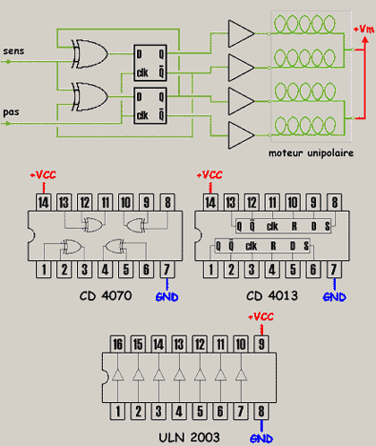 |
Pin Assignments for CD4093
Components list
IC :
quad. XOR = CD 4070 or 4030 Dual shift register = CD 4013 Ampli = ULN 2003 Unipolar stepper motor |
|
Stepper motors can be found on old floppy
disk drives or printers for example. In certain cases we can even use
the controllers who are joined to it. 2 control pulses can result from a
microcomputer (parallel port) + line buffers.
| ||
Monday, 13 February 2012
Stepper motor drive
Analogic / Digital converter
Analogic / Digital converter
This integrated circuit (AD
7821) allows to convert an analogic signal in a 8 bits value with a 1 µs
conversion time, thus with a 1 MHz frequency. There are faster
converters allowing to obtain a better resolution (10, 12, 14 or 16
bits).
|
||
|
Pin Assignments for AD7821
|
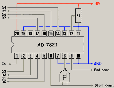 |
Components List
Pot. : P1 = 20 kΩ
A/D Converter = AD7821 trigger inverter = 1/4 CD4093 |
|
The signal resulting from the amplifier is
applied to the pin 1 (Input). The reference voltage is adjusted by
means of P1. It is very summary but that works. We can also use a
specific component to obtain this reference voltage (zener diode for
ex.).
The pulse "start of conversion" results
from the clock generator (having a 5 V level compatible with the
converter) and the pulse "End of conversion" is sent to the PC
interface, as well as 8 bits data. We can also send these data through
buffer circuits (74245 by eg) to secure the exchanges
interface-converter. The logic gate (1/4 CD4093) can be another
inverter.
| ||
Changing the pulse width
Changing the pulse width
The previous assembly gives a rectangular
signal with a duty cyclic equal to 50
%. We can need to change it
to produce pulses for example. A simple means is to use
a variable RC circuit and to reshape the signal obtained
by means of a Schmidt trigger , here a CD 4093 which
allows to use a wide range of voltage. (The CD 4093 is in
fact a quadruple logic gates NAND which we use here only
the inverter function).
|
||
|
Pin Assignments for CD4093
|
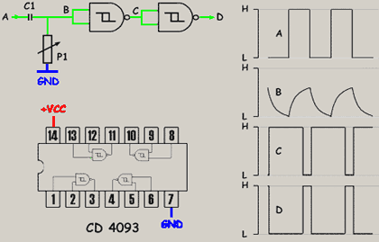 |
Components List
Pot. : P1
= 20 kΩ
Capacitors : C1, 33 pF digital circuit : CD 4093
Power supply VCC : 5 to 18 V
|
|
Modifying the value of P1 we make vary the height
of the signal (B) which is not any more squarewave but sawtooth.
The trigger activates when a threshold is reached
and we so obtain a modified duty cycle (C and D).
| ||
Clock pulse generator / binary counter
Clock pulse generator / binary counter
This digital circuit (CD
4060) allows to produce a stable square signal of high frequency by
means of a quartz and very few secondary components. Its counter
function (divide by 2 counter) allows to find one frequencies suited for
the clocks of the CCD.
|
||
|
Pin Assignments for CD4060
|
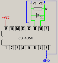 |
Components List
Resistor : R1 = 10 MΩ
Capacitors : C1, C2 = 4.7 pF Quartz : X1 = 12 MHz digital circuit : CD 4060
Power supply VCC : 5 to 18 V
|
|
Output Qi delivers a frequency equal to the quartz frequency divided by 2 at the power i (ex: Q5 gives Freq / 32)
| ||
Stepper Motor
Stepper Motor Data
program shows the basic operation of the stepper motors
 This program shows the basic operation of the unipolar and
bipolar stepper motors. In addition there are demos of a translator
, oscillator and indexer.http://www.wimb.net/index.php?s=delphi&page=6
Basic theory of Stepping Motors
Stepping motors are electromagnetic, rotary, incremental devices
which convert digital pulses into mechanical rotation. The amount
of rotation is directly proportional to the number of pulses and the
speed of rotation is relative to the frequency of those pulses.
 Static or holding torque - displacement characteristic
The characteristic of static (holding) torque - displacement is best
explained using an electro-magnet and a single pole rotor . In
the example the electro-magnet represents the motor stator and is
energized with it's north pole facing the rotorhttp://www.sapiensman.com/step_motor/
Stepper Motors: Principles of Operation

Permanent Magnet stepper motors incorporate a permanent magnet
rotor, coil windings and magnetically conductive stators. Energizing
a coil winding creates an electromagnetic field with a north and south
pole .
Switch-Mode Battery Charger Circuit
Switch-Mode Battery Charger Circuit
Fast, High Effi ciency, Standalone NiMH/NiCd Battery
Charging Circuit

Figure 1 shows a fast, 2A charger featuring the
high effi ciency LTC4011 550kHz synchronous buck
converter. The LTC4011 simplifi es charger design by
integrating all of the features needed to charge Ni-based
batteries, including constant current control circuitry,
charge termination, automatic trickle and top off
charge, automatic recharge, programmable timer,
PowerPath control and multiple status outputs. Such a
high level of integration lowers the component count,
enabling a complete charger to occupy less than 4cm2
of board area.
Battery Charger Delivers 2.5A With >96% EfficiencyBattery chargers are usually designed without regard for
efficiency, but the heat generated by low-efficiency
chargers can present a problem. For those applications,
the charger of Figure 1 delivers 2.5A with efficiency as
high as 96%. It can charge a battery of one to six cells
while operating from a car battery.

Figure 1. Modified feedback paths transform this switch-mode
power-supply circuit for notebook computers into a
high-efficiency battery charger.
WIDER POSITION SENSING CIRCUIT
WIDER POSITION SENSING CIRCUIT
To go from 45° to 90° requires two HMC1501
sensors or a single HMC1512 dual sensor part. By
using two bridges with 45° displacement from each
other, the two linear slopes can be used additively.
Figure 8 shows a typical configuration.
From Figure 8, as the shaft rotates around, magnetic
flux from a magnet placed at the end of the shaft exits
the north pole and returns to the south pole. With a
HMC1512 placed on the shaft axis, just above the
magnet, the flux passing through the sensor bridges
will retain the orientation of the magnet. From this
rotation, the output of the two bridges will create sine
and cosine waveforms as shown in Figure 9.


Because the sine (sensor bridge A) and cosine
(sensor bridge B) will match after the offset error
voltages are subtracted, the ratio of bridge A to bridge
B creates a tangent 2O function and the amplitude A
values cancel. Thus the angle theta is described
as:
(sensor bridge B) will match after the offset error
voltages are subtracted, the ratio of bridge A to bridge
B creates a tangent 2O function and the amplitude A
values cancel. Thus the angle theta is described
as:
 However because there are some trigonometric
nuances with the arctangent function when gets
close to _45° and beyond, these special cases apply:
 Because most trigonometric functions are performed
as memory maps in microcontroller integrated circuits,
these kinds of special case conditions are easily dealt
with. The resultant angle theta is the relative
position of the magnetic field with respect to the
sensor. It should be noted that if rotation is permitted
beyond _90°, the theta calculation will replicate again
with postive and negative 90° readings jumping at the
end points. Further performance to 360° or _180° can
be mapped into a microcontroller by using this circuit
plus a Hall Effect sensor to determine which side of
the shaft is being positionally measured via magnetic
polarity detection. Figure 10 shows the basic circuit
interface for the HMC1512.

Source http://www.ssec.honeywell.com/magnetic/datasheets/an211.pdf
HMC1501 / HMC1512
Linear / Angular / Rotary
Displacement Sensors
High resolution, low power MR sensor capable of measuring the angle
direction of a magnetic field from a magnet with <0.07>
HMC1501 / HMC1512
Linear / Angular / Rotary
Displacement Sensors
High resolution, low power MR sensor capable of measuring the angle
direction of a magnetic field from a magnet with <0.07>
LCDs connected to the micro Controller
LCDs connected to the uC
LCDs connected to the microcontroller in 4 bit data bus mode. LCD will require
a total of 7 data lines
3 control lines plus the 4 lines for the data bus in simple control LCD we will set
RW = 0(write only)
- The EN line is called "Enable."
This control line is used to tell the LCD that you are sending it data.
- The RS line is the "Register Select" line.
RS is low (0), the data is to be treated as a command or special instruction
RS is high (1), the data being sent is text data which sould be displayed on the
screen.
- The RW line is the "Read/Write" control line.
RW is low (0), the information on the data bus is being written to the LCD.
RW is high (1), the program is effectively querying (or reading) the LCD.

LM231
LM231
The LM231/LM331 family of voltage-to-frequency converters
are ideally suited for use in simple low-cost circuits for
analog-to-digital conversion, precision frequency-to-voltage
conversion, long-term integration, linear frequency modulation
or demodulation, and many other functions
Features
- Guaranteed linearity 0.01% max
- Improved performance in existing voltage-to-frequency
conversion applications
- Split or single supply operation
- Operates on single 5V supply
- Pulse output compatible with all logic forms
- Excellent temperature stability, ±50 ppm/°C max
- Low power dissipation, 15 mW typical at 5V
- Wide dynamic range, 100 dB min at 10 kHz full scale
- Wide range of full scale frequency, 1 Hz to 100 kHz
- Low cost
Remote I/O expander circuit
Remote I/O expander circuit
Each of the PCF8574’s eight I/Os can be independently
used as an input or output.
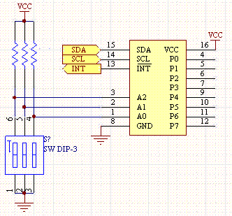
PCF8574Remote 8-bit I/O expander for I2C-bus
The PCF8574 is a silicon CMOS circuit. It provides general
purpose remote I/O expansion for most microcontroller
families via the two-line bidirectional bus (I2C).
The device consists of an 8-bit quasi-bidirectional port and
an I2C-bus interface. The PCF8574 has a low current
consumption and includes latched outputs with high
current drive capability for directly driving LEDs. It also
possesses an interrupt line (INT) which can be connected
to the interrupt logic of the microcontroller. By sending an
interrupt signal on this line, the remote I/O can inform the
microcontroller if there is incoming data on its ports without
having to communicate via the I2C-bus. This means that
the PCF8574 can remain a simple slave device.
Address of PCF8574 can set at pin A0,A1,A2
slave addresses.
Simple Large Fan-In AND Gate circuit
Simple Large Fan-In AND Gate circuit
We can make simple Large Fan-In AND Gate circuit by one Voltage
Comparators from circuit below
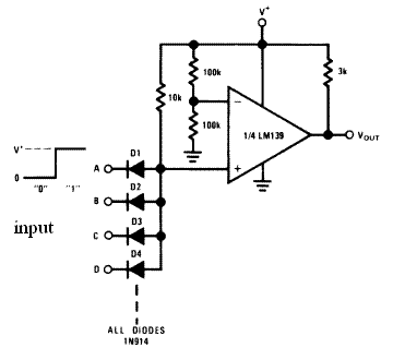
Vout = A and B and C and D and ….
This circuit is application of LM139
LM139
Low Power Low Offset Voltage Quad Comparators
The LM139 series consists of four independent precision
voltage comparators with an offset voltage specification as
low as 2 mV max for all four comparators. These were
designed specifically to operate from a single power supply
over a wide range of voltages.
All pins of any unused comparators should be tied to the
negative supply.
The output of the LM139 series is the uncommitted collector
of a grounded-emitter NPN output transistor. Many collectors
can be tied together to provide an output OR’ing function.
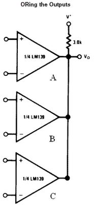
Vo = A or B or C
5A switching regulator with Adjustable Current Limit
5A switching regulator with Adjustable Current Limit

LM26795A Step-Down Voltage Regulator
with Adjustable Current Limit
with Adjustable Current Limit
DescriptionThe LM2679 series of regulators are monolithic integrated
circuits which provide all of the active functions for a stepdown
(buck) switching regulator capable of driving up to 5A
loads with excellent line and load regulation characteristics.
High efficiency (>90%) is obtained through the use of a low
ON-resistance DMOS power switch. The series consists of
fixed output voltages of 3.3V, 5V and 12V and an adjustable
output version.
The SIMPLE SWITCHER concept provides for a complete
design using a minimum number of external components. A
high fixed frequency oscillator (260KHz) allows the use of
physically smaller sized components. A family of standard
inductors for use with the LM2679 are available from several
manufacturers to greatly simplify the design process.
Other features include the ability to reduce the input surge
current at power-ON by adding a softstart timing capacitor to
gradually turn on the regulator. The LM2679 series also has
built in thermal shutdown and resistor programmable current
limit of the power MOSFET switch to protect the device and
load circuitry under fault conditions. The output voltage is
guaranteed to a ±2% tolerance. The clock frequency is
controlled to within a ±11% tolerance.
Features- Efficiency up to 92%
- Simple and easy to design with (using off-the-shelf
external components)
- Resistor programmable peak current limit over a range
of 3A to 7A.
- 120 mΩ DMOS output switch
- 3.3V, 5V and 12V fixed output and adjustable (1.2V to
37V ) versions
- ±2%maximum output tolerance over full line and load
conditions
- Wide input voltage range: 8V to 40V
- 260 KHz fixed frequency internal oscillator
- Softstart capability
- −40 to +125°C operating junction temperature range
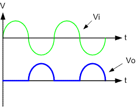
Half-wave precision rectifiers circuit
Half-wave precision rectifiers circuit
A half-wave rectifier is a circuit that passes only the positive or only the negative
Portion of a wave ,while blocking out the other portion
Rectifiers are impremented using diodes. The nonzero forward-voltage drop of
A pactical diode may cause intolerable errors in low-level signal
Proceeding of half-wave precision rectifiers circuit we separate are two case
Case 1 Vi > 0 negative input of op amp is higher positive input ,the op amp
Output = 0 ,I1 will flow through R1 and D1 ,hence Vo = 0
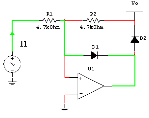
Case 2 Vi <>
Output = 1 ,I2 will flow through R2,R1 and D2 ,but the voltage at positive input
Must equal the voltage at negative input ,hence I2 = (0-Vi)/R1 = (Vo-0)/R2
This gives Vo = (-R2/R2)Vi
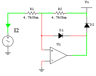
Circuit behaviorVo = 0 for Vi > 0
Vo = -(R2/R1)Vi for Vi <>
Example waveform
PWM Generator with Current Limit Circuit
PWM Generator with Current Limit Circuit
 SG3524
The SG2524 and SG3524 incorporate all the
functions required in the construction of a
regulating power supply, inverter, or switching
regulator on a single chip. They also can be used
as the control element for high-power-output
applications. The SG2524 and SG3524 were
designed for switching regulators of either polarity,
transformer-coupled dc-to-dc converters, transformerless
voltage doublers, and polarity converter applications
employing fixed-frequency, pulse-width-modulation
(PWM) techniques. The complementary output allows
either single-ended or push-pull application. Each device
includes an on-chip regulator, error amplifier, programmable
oscillator, pulse-steering flip-flop, two uncommitted
pass transistors, a high-gain comparator, and current-limiting
and shut-down circuitry.
12-Bit A/D Converter
12-Bit A/D Converter
MCP320212-Bit A/D Converter with SPI® Serial InterfaceThe Microchip Technology Inc. MCP3202 is a successive
approximation 12-bit Analog-to-Digital (A/D) Converter
with on-board sample and hold circuitry. The
MCP3202 is programmable to provide a single
pseudo-differential input pair or dual single-ended
inputs.
FEATURES
• 12-bit resolution
• ±1 LSB max DNL
• ±1 LSB max INL (MCP3202-B)
• ±2 LSB max INL (MCP3202-C)
• Analog inputs programmable as single-ended or
pseudo-differential pairs
• On-chip sample and hold
• SPI® serial interface (modes 0,0 and 1,1)
• Single supply operation: 2.7V - 5.5V
• 100ksps max. sampling rate at VDD = 5V
• 50ksps max. sampling rate at VDD = 2.7V
• Low power CMOS technology
- 500nA typical standby current, 5μA max.
- 550μA max. active current at 5V
• Industrial temp range: -40°C to +85°C
• 8-pin PDIP SOIC and TSSOP packages
MCP3202 Datasheet pdf
4-to-16 Decoder IC
4-to-16 Decoder IC
MM74HC154
New product of fairchild semoconductor
The MM74HC154 decoder utilizes advanced silicon-gate
CMOS technology, and is well suited to memory address
decoding or data routing applications. It possesses high
noise immunity, and low power consumption of CMOS with
speeds similar to low power Schottky TTL circuits.
The MM74HC154 have 4 binary select inputs (A, B, C, and
D). If the device is enabled these inputs determine which
one of the 16 normally HIGH outputs will go LOW. Two
active LOW enables (G1 and G2) are provided to ease
cascading of decoders with little or no external logic.
2.5 V Voltage References IC
2.5 V Voltage References IC
MCP1525 2.5 V Voltage References IC
 Description
 The Microchip Technology Inc. MCP1525/41 devices
are 2.5V and 4.096V precision voltage references that
use a combination of an advanced CMOS circuit
design and EPROM trimming to provide an initial
tolerance of ±1% (max.) and temperature stability of
±50 ppm/°C (max.). In addition to a low quiescent
current of 100 μA (max.) at 25°C, these devices offer a
clear advantage over the traditional Zener techniques
in terms of stability across time and temperature. The
output voltage is 2.5V for the MCP1525 and 4.096V for
the MCP1541. These devices are offered in SOT-23-3
and TO-92 packages, and are specified over theindustrial
temperature range of -40°C to +85°C.
Features• Precision Voltage Reference
• Output Voltages: 2.5V and 4.096V
• Initial Accuracy: ±1% (max.)
• Temperature Drift: ±50 ppm/°C (max.)
• Output Current Drive: ±2 mA
• Maximum Input Current: 100 μA @ +25°C (max.)
• Packages: TO-92 and SOT-23-3
• Industrial Temperature Range: -40°C to +85°C
20-Bit ADC which digital filters
20-Bit ADC which digital filters
CS5526CS5526 are highly integrated A/D converters which include
An instrumentation amplifier, a PGA (programmable gain
amplifier), eight digital filters, and self and system calibration
circuitry.

The converters are designed to provide their own negative
supply which enables their on-chip instrumentation
amplifiers to measure bipolar ground-referenced signals
±100 mV. By directly supplying NBV with -2.5 V and
with VA+ at 5 V, 2.5 V signals (with respect to ground)
can be measured.
Features
lDelta-Sigma A/D Converter
- Linearity Error: 0.0015%FS
- Noise Free Resolution: 18-bits lBipolar/Unipolar
- 25 mV, 55 mV, 100 mV, 1 V, 2.5 V and 5 V
lChopper Stabilized Instrumentation Amplifier
lOn-Chip Charge Pump Drive Circuitry
l4-Bit Output Latch
lSimple three-wire serial interface
- SPI™ and Microwire™ Compatible
- Schmitt Trigger on Serial Clock (SCLK)
lProgrammable Output Word Rates
- 3.76 Hz to 202Hz (XIN = 32.768 kHz)
- 11.47 Hz to 616 Hz (XIN = 100 kHz)
lOutput Settles in One Conversion Cycle
lSimultaneous 50/60 Hz Noise Rejection
lSystem and Self-Calibration with
Read/Write Registers
lSingle +5 V Analog Supply
+3.0 V or +5 V Digital Supply
lLow Power Mode Consumption: 4 mW
- 1.8 mW in 1 V, 2.5 V, and 5 V Input Ranges
True RMS-to-DC IC
True RMS-to-DC IC
MX536A and MX636Maxim-ICThe MX536A and MX636 are true RMS-to-DC converters.
They feature low power and are designed to accept
low-level input signals from 0 to 7VRMS for the MX536A
and 0 to 200mVRMS for the MX636. Both devices accept
complex input waveforms containing AC and DC components.
They can be operated from either a single supply
or dual supplies. Both devices draw less than 1mA
of quiescent supply current, making them ideal for battery-
powered applications.

Feature- True RMS-to-DC Conversion
- Computes RMS of AC and DC Signals
- Wide Response:
2MHz Bandwidth for VRMS > 1V (MX536A)
1MHz Bandwidth for VRMS > 100mV
- Auxiliary dB Output: 60dB Range (MX536A)
50dB Range (MX636)
- Single- or Dual-Supply Operation
- Low Power: 1.2mA typ (MX536A)
800μA typ (MX636)
Protected 2A Switch circuit
Protected 2A Switch circuit
Protected 2A Switch with Isolated Inputs , Fault Output circuit
 LT1161
The LT1161 is a quad high-side gate driver allowing the
use of low cost N-channel power MOSFETs for high-side
switching applications. It has four independent switch
channels, each containing a completely self-contained
charge pump to fully enhance an N-channel MOSFET
switch with no external components.
Features
- Fully Enhances N-Channel MOSFET Switches
- 8V to 48V Power Supply Range
- Protected from –15V to 60V Supply Transients
- Individual Short-Circuit Protection
- Individual Automatic Restart Timers
- Programmable Current Limit, Delay Time, and
Auto-Restart Period
- Voltage-Limited Gate Drive
- Defaults to OFF State with Open Input
- Flowthrough Input to Output Pinout
- Available in 20-Lead DIP or SOL Package
Overcurrent Protection Circuit
Overcurrent Protection Circuit
Overcurrent Protection Circuit for High Side Relay Diver
 LTC1154
The LTC1154 single high side gate driver allows using low
cost N-channel FETs for high side switching applications. An
internal charge pump boosts the gate drive voltage above
the positive rail, fully enhancing an N-channel MOS switch
with no external components. Micropower operation, with
8μA standby current and 85μA operating current, allows
use in virtually all systems with maximum effi ciency.
Included on chip is programmable overcurrent sensing.
A time delay can be added to prevent false triggering on
high inrush current loads.
Feature
- Fully Enhances N-Channel Power MOSFETs
- 8μA IQ Standby Current
- 85μA IQ ON Current
- No External Charge Pump Capacitors
- 4.5V to 18V Supply Range
- Short-Circuit Protection
- Thermal Shutdown via PTC Thermistor
- Status Output Indicates Shutdown
- Available in 8-Pin SOIC and PDIP Packages
Bidirectional Current Sensor
Bidirectional Current Sensor
Bidirectional Hall Effect Based Linear Current Sensor with
Voltage Isolation and 20 A Dynamic Range
ACS706ELC-20A
 The Allegro ACS706 family of current sensors provides economical
And precise solutions for current sensing in industrial, automotive,
commercial, and communications systems. The device package allows
for easy implementation by the customer. Typical applications include
motor control, load detection and management, switched-mode power
supplies, and overcurrent fault protection.
Current Input Range Min -20 A Max 20 A
Output Voltage versus Current Input (Vcc = 5V)
 Features
• Small footprint, low-profile SOIC8 package
• 1.5 mΩ internal conductor resistance
• Excellent replacement for sense resistors
• 1600 VRMS minimum isolation voltage between pins 1-4 and 5-8
• 4.5 to 5.5 V, single supply operation
• 50 kHz bandwidth
• 100 mV/A output sensitivity and 20 A dynamic range
• Output voltage proportional to ac and dc currents
• Factory-trimmed for accuracy
• Extremely stable output offset voltage
• Near-zero magnetic hysteresis
• Ratiometric output from supply voltage
Power MOSFET Drivers Circuit
Power MOSFET Drivers Circuit
1.5A Dual High-Speed Power MOSFET Drivers

The TC4426A/TC4427A/TC4428A are improved
versions of the earlier TC4426/TC4427/TC4428 family
of MOSFET drivers. In addition to matched rise and fall
times, the TC4426A/TC4427A/TC4428A devices have
matched leading and falling edge propagation delay
times.
Features:- High Peak Output Current – 1.5A
- Wide Input Supply Voltage Operating Range: 4.5V to 18V
- High Capacitive Load Drive Capability – 1000 p in 25 ns (typ.)
- Short Delay Times – 30 ns (typ.)
- Matched Rise, Fall and Delay Times
- Low Supply Current:
- With Logic ‘1’ Input – 1 mA (typ.)
- With Logic ‘0’ Input – 100 μA (typ.)
- Low Output Impedance – 7Ω (typ.)
- Latch-Up Protected: Will Withstand 0.5A Reverse Current
- Input Will Withstand Negative Inputs Up to 5V
- ESD Protected – 4 kV
- Pin-compatible with TC426/TC427/TC428 and
TC4426/TC4427/TC4428
- Space-saving 8-Pin MSOP and 8-Pin 6x5 DFN Packages
PWM using 555
PWM using 555

IC1 astable gives a fixed square wave at pin 3, C1 and R1 derive
uS trigger pulses from IC1 and this will trigger IC2 monostable or
single shot, the voltage at pin 5 of IC2 will change the pulse width
output of IC2, to get it working all the three RC combinations
have to be figured out
PWM Generator Circuit by Digital register method
PWM Generator Circuit by Digital register method
 an example circuit using the digital comparison method
when a microcontroller is available to set the 4-bit digital register
value. A write strobe is required from the micro to latch the 4 data
bits into the register. The 74HC161 counter is free-running,
the frequency being set by the 74HC14 oscillator section, where
it is roughly f = 1/(6.3RC). The resulting frequency of the PWM
signal will be 16 times less than this counter clock frequency,
since it requires 16 pulses to complete one "revolution" of the
counter. With R=2k and C=1nF this results in a counter
frequency of approximately 80kHz which will result in a PWM signal
frequency of 5kHz.
Opamp PWM Generator Circuit
Opamp PWM Generator Circuit


This uses the LM324, a 14-pin DIL IC containing four individual
op-amps and running off a single-rail power supply.
The sawtooth is generated with two of them (U1A and U1B),
configured as a Schmitt Trigger and Miller Integrator, and
a third (U1C) is used as a comparator to compare the sawtooth
with the reference voltage and switch the power transistor.
op-amps and running off a single-rail power supply.
The sawtooth is generated with two of them (U1A and U1B),
configured as a Schmitt Trigger and Miller Integrator, and
a third (U1C) is used as a comparator to compare the sawtooth
with the reference voltage and switch the power transistor.
PWM Generator Circuit
PWM Generator Circuit
PWM generator

Here is an assembly very simple to get an oscillator giving
a fixed frequency signal but variable duty cycle. It can - after
amplifier transistor - serve to control the rotation speed of a motor
with direct current or to adjust the power of a dew-heater. We use
once again a logic gate of a CD4093 circuit.
a fixed frequency signal but variable duty cycle. It can - after
amplifier transistor - serve to control the rotation speed of a motor
with direct current or to adjust the power of a dew-heater. We use
once again a logic gate of a CD4093 circuit.
A Simple PWM Circuit Based on the 555 Timer
A Simple PWM Circuit Based on the 555 Timer


The 555 timer in the PWM circuit is configured as an astable
oscillator. This means that once power is applied, the 555 will
oscillate without any external trigger. Before the technical
explanation of the circuit, let's look at the 555 timer IC itself.
oscillator. This means that once power is applied, the 555 will
oscillate without any external trigger. Before the technical
explanation of the circuit, let's look at the 555 timer IC itself.
Implementation USB into AVR microcontroller
Implementation USB into microcontroller: IgorPlug-USB (AVR)

Purpose of this article is to inform readers about
implementation USB interface into singlechip microcontroller, which this
interface directly not supports. Simply: implementation USB interface on
firmware level (similar as emulation of RS232 interface in microcontrollers,
which not have RS232 support). This project includes development of firmware on
microcontroller side, driver development on computer side (for Windows operating
system) , development of DLL library for functions calling from another programs
(programmers level) and development of demo program (users level), which shows
all functions of this device. Device is named IgorPlug-USB (AVR) (as
successor of my previous device for computer remote control IgorPlug
- serial port version).Introduction:
At present time is USB interface very popular especially within end user. This is due to the simplicity to the end users (Plug and Play, without restart). For developers is implementation of USB into their devices more complicated (with comparison to RS232 is USB more complex protocol). In addition there is need of software support on PC side - device drivers. Therefore more devices from small vendors are inclined to RS232 communication. This interface is probably the oldest in PC history and has good operating system support. But in latter years is RS232 removing from standard included PC interfaces (new computers hasn't RS232). In this case help only add-on PCI card with this interface.Implementation of USB into external devices is at present time solved in two choices:
a) First is using microcontroller, which have hardware implemented USB interface. Then is necessary to know how USB works and according this write firmware into microcontroller. And in addition is necessary to create driver on the computer side (while operating system not includes it - e.g. standard USB classes). Disadvantage (and this is the main disadvantage for small vendors and amateurs) is not good availability of this microcontrollers (PIC, Cypress, Atmel, Intel, ...) and their high price (with comparison to simple "RS232" microcontrollers).
b) Second option is to use some universal converter between USB and "another" interface. This "another" interface depends on type of convertor: there are used especially RS232, 8-bit data bus, I2C bus. In this case is not need of special firmware (actually we needn't to know how USB works) and no need of driver writing (vendor of converter offer free drivers). Disadvantage is higher price of the complete device and greater dimensions of product (need of one chip more).
My solution,
which I have resolved to develop - and successfully finished ;-) - is
USB implementation into cheap microcontroller through the emulation of USB
protocol in firmware of microcontroller. Problem during design
was microcontroller speed. Speed of USB bus is too high: LowSpeed - 1.5Mbit/s,
FullSpeed - 12Mbit/s, HighSpeed - 480Mbit/s. Normal microcontrollers are maximum
performance cca: AT89C2051 - 2MIPS = 24MHz/(12cycl/inst.), PIC16F84 - 5MIPS =
20MHz/(4cycl/inst.), AT90S23x3 - 10MIPS = 10MHz/(1cycl/inst.). There exist
microcontrollers with highest speeds too, but they are poorly available (price
too) and are biggest (more pins - difficult construction). For all that I have
decided for microcontrollers PIC16F84 or AT90S1200/AT90S23x3, which would be
"enough" for LowSpeed USB. For highest USB speeds is this solution not
good - for one bit from USB processing is need of several cycles of
microprocessor: reading, comparison, storing, some operation, ... .
Firstly I choose PIC16F84-20, with which I have experiences. To ensure synchronizing with USB clock and speed increasing was used microcontroller clock 24MHz = 6MIPS (PIC was slightly overclocked). For one bit from USB processing were 4 instructions (4=6MIPS/1.5Mbit for LowSpeed USB). I reject this solution (after some time) - PIC is too slow (and in addition the no so good instruction set ...) .
Second try was AT90S1200-12, which satisfied me with its speed - possible to receive and transmit signal on LowSpeed USB speed. But I reject this solution too - absence of enough program and data memory - simply small memory to implement this.
Third try was successful: AT90S2313-10 (or AT90S2323-10, AT90S2343-10). This are RISC microcontrollers from Atmel production - AVR family. With comparison with PIC are slow crystal clock, but have 1 instruction per crystal clock (PIC16F84 has to 1 instruction per 4 crystal clock). In addition their instruction set and architecture is nearly to RISC. Again because of synchronization with USB clock I used overclocking to12MHz (AT90S23x3-10 are initially to10MHz only). In this manner I obtained more performance and 12MHz crystals are "easy to obtain" (with comparison to e.g. 10.5MHz - which is the multiple of LowSpeed USB clock 1.5Mbit/s too).
Construction:
My solution offer very simple and cheap hardware (cca 3,-US$). All intelligence is in firmware. Construction is designed as infrared remote control of computer through USB (successor of construction for serial port ), but this is universal USB interface too.This device allow:
- receiving of infrared code (time diagram of received code) (it is transmitted to serial line in real time too) (receiving of infrared code makes microprocessor without PC - zero usage of PC CPU)
- control of 8-bit input-output data gate (every bit can be independently input or output, there can be independently controlled pull-up resistors on input pins)
- reading and writing of internal 128 byte EEPROM (storing of data after no power state - for users is accessible all memory)
- transmitting or receiving char via serial line
(now only one non buffered char - but by firmware change is possible to make internal buffer (for injury of infra buffer) : like FTDI chips) - change of baudrate of serial line in range cca
4800Baud to 700 000Baud (after power on is 57600baud)
("Classical" baudrates are: 4800, 9600,19200,38400,57600. Device DLL automatically detects invalid baudrates.)
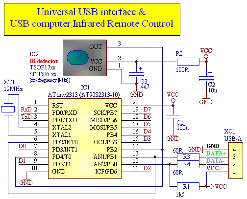
On the next picture is schematic:
with microprocessor AT90S2313-10 (universal interface):
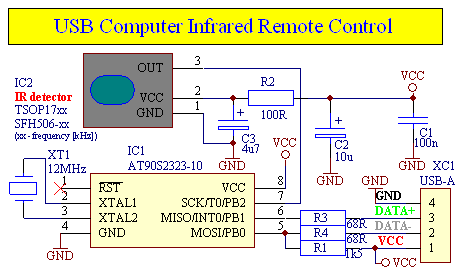
or with microprocessor AT90S2323-10 (only for IR code receiving) - not tested yet, but designed for this purpose - was tested by users - WORKS GOOD:
and physical construction (IR receiver: computer remote control for program Girder):
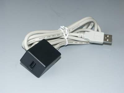
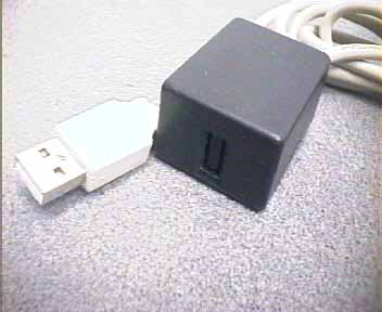
Simplicity of device is truly wondrous. And is accessible for amateurs too - for their devices connection to USB (this always enjoy - I know this according my experience, when Windows first time find this "New hardware found" ;-) ). Firmware - the heart of device - is the same for both microprocessors. In 8-pin version (AT90S2323-10) you can use only infrared code receiving and writing/reading to/from EEPROM. But 8-pin version is by dimension probably the smallest device connected to USB (SMD version).
Installation of device IgorPlug-USB (AVR):
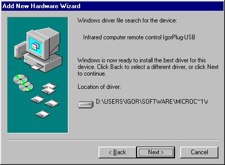
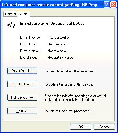
For success communication between USB device and computer, there is necessary to give driver for device. This driver is requested by operating system during first connection IgorPlug-USB (AVR) into USB connector in computer. In the future maybe this driver will not be necessary : by change in firmware is possible, that device will be standard USB class (HID class, Storage Class ,...), - for this classes has operating system build-in drivers. Advantage of own driver is, that we have control of driver behavior. I choose for "own" driver only because of learning "how this works" and mainly for simplicity of implementation into firmware of device.Next pictures shows device installation steps (and driver installation) on the first plugging IgorPlug-USB (AVR) into USB connector. Driver is the same for Windows98, WindowsME, Windows2000 and WindowsXP (under Windows95 not works):
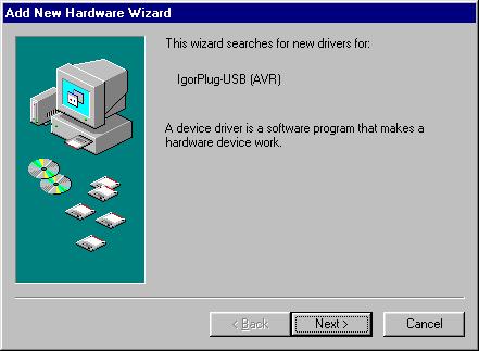
Firstly under WindowsXP:
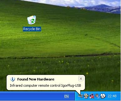
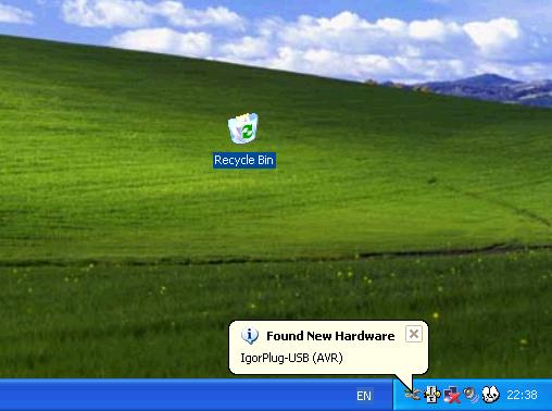 Windows find device IgorPlug-USB (AVR).
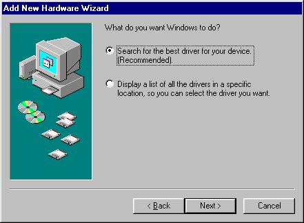
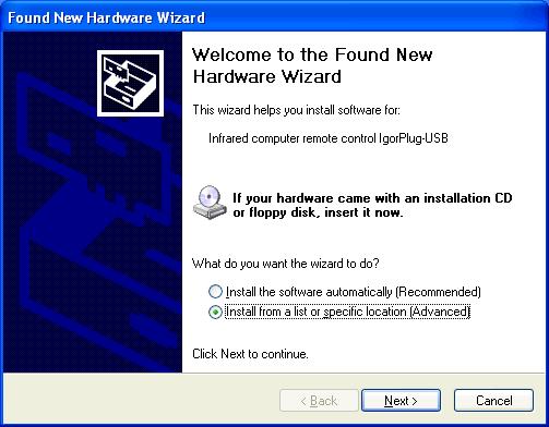 Choose install from our location.
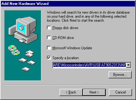
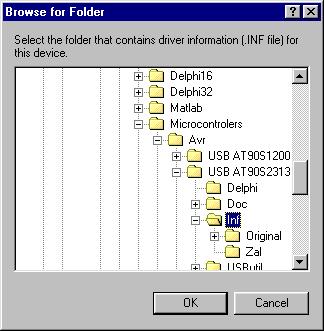
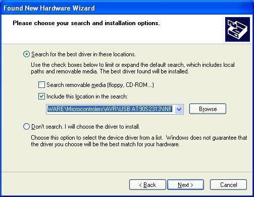 Here we browse to folder with installation files (INF file and SYS driver)
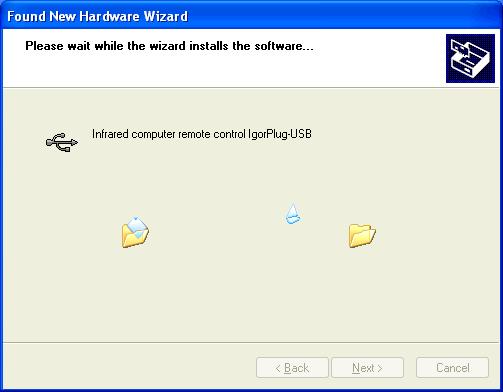 Windows
do some necessary changes.
Windows
do some necessary changes.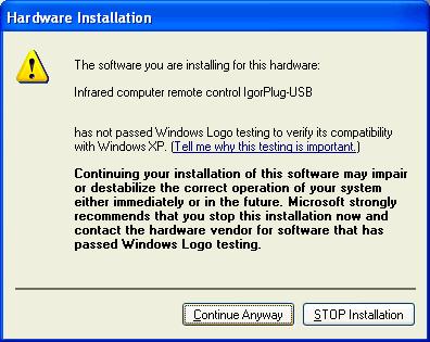 Driver have not digital signature from Microsoft - but we not stop installation.
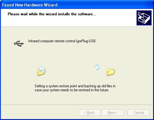 Windows make backup (for safe recovery ;-) ).
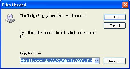 And in case when Windows don't to find SYS driver, ...
 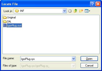 ... then we give to him correct path to driver.
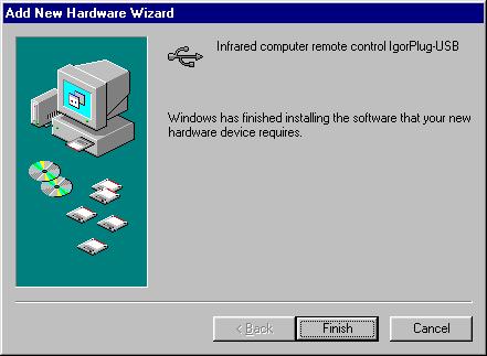
 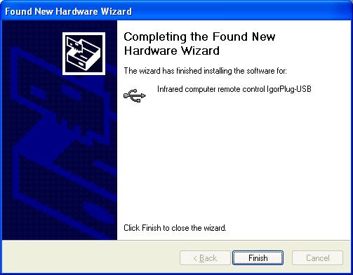 And installation is finished:
And under Windows98:
The same as under WindowsXP, only in another visual form.
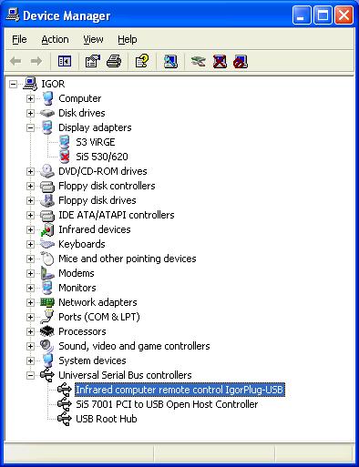
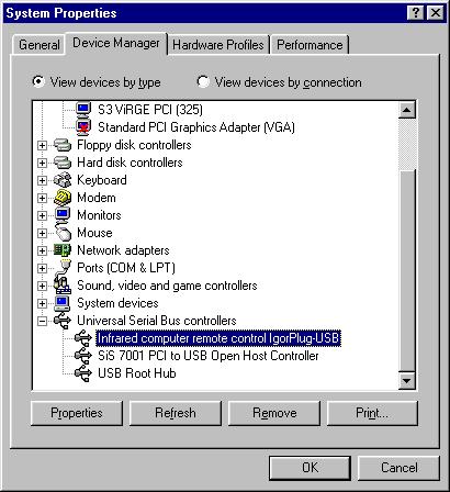
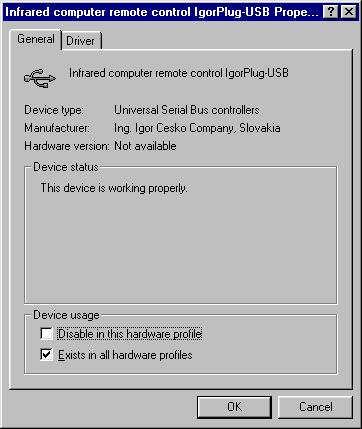
After success installation we can look at device in "Device manager":
Device Manager under WindowsXP:
Device Manager under Windows98:
Software support:
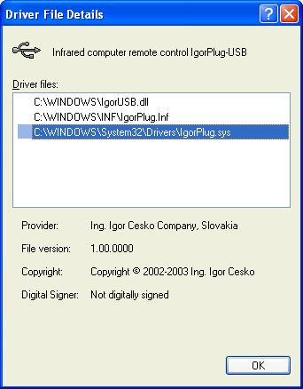
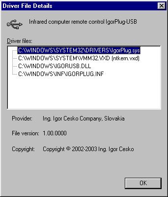
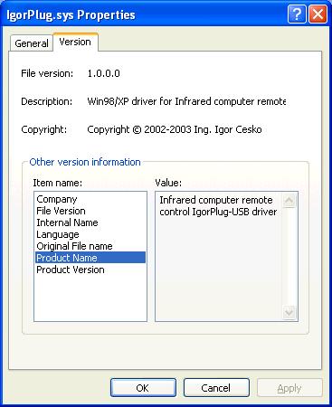
As I mentioned - for correct device operation is necessary driver, which is requested by operating system during installation. This driverFor installation is necessary installation descriptive file INF. Just this file was requested by Windows during installation of device and we must browse to folder with this INF file if we are asked for driver location. In this file is install information for given device - and according to this information will be installed driver and eventually will be made other actions. I was created this INF file according to template file from my USB book. Because every USB device must have assigned vendor number (VID) from USB-organization (USB-IF), then I "borrow" this number from company Atmel (I hope that Atmel excuse me this borrowing - I won't to pay cca 1500 US$ for number assignment) and I implement it into microprocessor and into INF file. Name of this file is "IgorPlug.inf" and is included in installation pack. So for device installation are necessary only two files ("IgorPlug.sys" a "IgorPlug.inf").
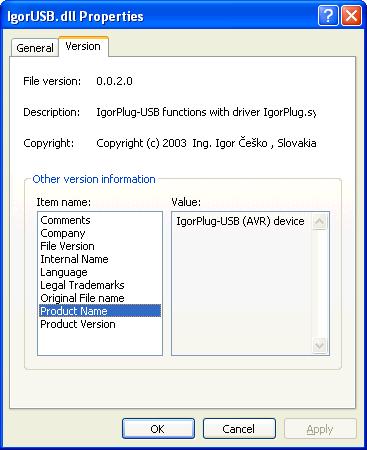
By this way we had successfully installed device IgorPlug-USB (AVR). And we can go to test it. For this purpose I had written DLL library "IgorUSB.dll", which contains functions, which device IgorPlug-USB (AVR) makes. This DLL library communicates with driver "IgorPlug.sys" and provide serialization of communication (when we are using DLL from more threads or applications). Library DLL is primary dedicated for programmers of end user applications for access to device: exported functions from DLL are published.
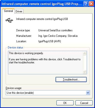
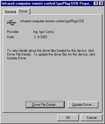
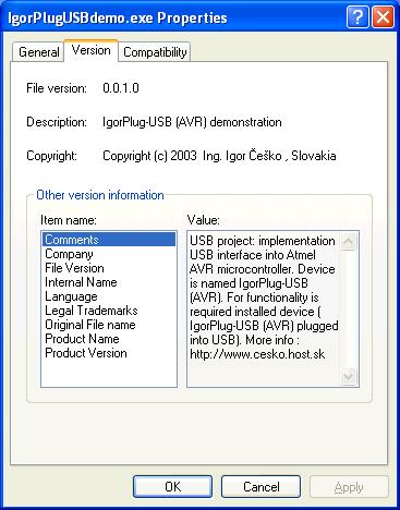
Next pictures shows information about DLL library and SYS driver as was displayed under WindowsXP:
Finally I had created end user application - exemplar program "AVR to USB tester", which shows all functions of device IgorPlug-USB (AVR). It call functions from DLL library "IgorUSB.dll" and is in fact the sample program.
Program functions:
- setting and reading of 8-bit data port (see schematic)
- port bits flow control and back reading of state of this flow control
- control of pull-up resistors on data pins (pull-up enabled, or high impedance input) and back reading of this state
- reading data pins level state (refresh every 200ms)
- setting LED diodes, which are connected to data pins through resistors (cathode on GND, is necessary to set all bits as outputs)
- reading data from all EEPROM
- writing data to all EEPROM
- writing - transmitting data to microprocessor serial line
- receiving char(s) from serial line (polling every 100ms)
- changing serial line baudrate (invalid baudrate - baudrate with error greater than 4% - is displayed as crossed number, unsuccessful set is signaled by red color in baudrate box)
- back reading of internal true baudrate (polling every 100ms)
- receiving of oscilloscopic record of infrared code received into internal
microprocessor buffer (refresh every 50ms)
(received infrared code is displayed in graphical form as on oscilloscope - its decoding must make another application)
(during infrared code receiving is this code transmitted to serial line too - but "on the fly" - therefore is necessary to set high baudrate of RS232 - therefore after power on is baudrate 57600 Baud)

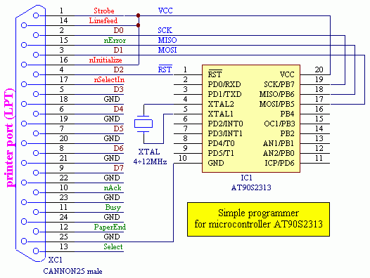
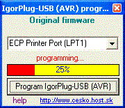
For programming AVR microcontroller is necessary programmer. But commercial programmer is for most users hard to obtain because its high price. Therefore I design simple LPT programmer of this microlontrollers - simple connection to computer LPT port. For this programmer I wrote control software - inside it is also firmware of device IgorPlug-USB (AVR) (only start program and burn microcontroller) and also schematics of programmer (for both microcontrollers: AT90S2313 and AT90S2323).
Here is schematic of programmer and its control program (works under WinXP too):
You can download control software in download section.
Something about development:
Development of this device was cca 4 months long (every evening after work cca 4 hours - long evenings ;-) ) + previous study and knowledge about USB and AVR microprocessors. Therefore this was not too easy (I must all study, watch, try alone). But now is no problem for me to change some function of microcontroller (e.g. omit "infra-buffer" and instead it to implement RS232 buffer). And USB is now nothing "unknown" for me (from the physical level to end user application).Idea of this project was in my head cca 2 years (after my first download of USB specification) - reborn was after similar project of one Russian "developer", which make this - but this was only his All Fools Day joke (but at that time I give the lie to his device). But his project was impulse for me to my project activity and to slogan : nothing is impossible ;-) .
The biggest "unknown" was understand all USB specification (but really all - from the physical level to end user level). Therefore study of USB was very important. The main information source was USB specification (free download from http://www.usb.org) and lately book "USB Měření, řízení a regulace pomocí sběrnice USB" from publisher BEN . And of course various internet sources.
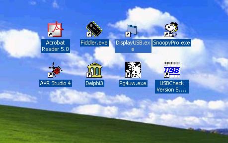
During development I was using for testing many "test" a "information utility" downloaded from internet (USBcheck, DisplayUSB, SnoopyPro, Fiddler, ...). For firmware development I was using free tool "AVR Studio 4" (from Atmel-u pages) and programmer "T51prog" (from Elnec company). For "physical observation" was used "Scopemeter FLUKE 123" (wonderful device) from FLUKE . As template design of USB device was for me USB mouse "Genius NetScroll+" from Genius company (bought in Agem-e). The microprocessor (and the "unsuccessful" too) I has bought in GM-electronic . So Many Thanks to all for help.
I was using for development next programs and many thanks of their creators:
And who want to see more pictures from my "development place" , here are: DevelopmentBoard1, DevelopmentBoard2, DevelopmentBoard3, DevelopmentBoard4, DevelopmentPlace1.JPG, DevelopmentPlace1, DevelopmentTools1, DevelopmentToolsElnecProgrammer, TargetDeviceAtmelAVR, TargetDeviceToUSBcable, LiteratureAndInformationSource.
And some information about my device IgorPlug-USB (AVR) as was dislayed by test utilities: USBDesignByExample, USBCheckFullTest, USBCheckDeviceDescriptor, USBCheckConfigurationDescriptor, USBCheckInterfaceDescriptor, USBCheckEndpointDescriptor, USBCheckViewDescriptors, USBCheck, SnoopyProDeviceDescriptor, SnoopyProConfigurationDescriptor, SnoopyProVendorCommand, ......enough (for unfamiliar persons are this not so clearly).
For the persons concerned to build this device as USB receiver like small USB key
 I prepared documentation: PCB layout, schematic and PCB devices
location. This documentation you can see here as
PDF file.
I prepared documentation: PCB layout, schematic and PCB devices
location. This documentation you can see here as
PDF file.Download:
Firmware into microprocessor is available in HEX-file and now also as source code (I publish it for more users requests - for adding your own functions). And now I publish documentation of PC software support (that was in the past only in full version). Of course: commercial use is not free. As freeware I publish e.g. computer remote control on serial port , (and all other my projects) and even if I was requesting small development fee from satisfied users, so from cca 20 000 downloads (about which I know) will be helpful only one person (4US$ - thank you) (although time for answering to cca 1500 e-mails is too much). So there is rule - if there is something free only per voluntary - no wait from anybody.Because I want that device will be available for more users, then for download is : IntelHEX file for AT90S23x3-10, driver , DLL-library for access to IgorPlug-USB (AVR) and demonstration program for control of IgorPlug-USB (AVR) (so all :-o ).
In the next I publish source code of firmware of microcontroller and also documentation of DLL library (for writing your own applications). Documentation is for Delphi, C++Builder/Visual C++, Visual Basic. So everybody can try how the device work.
For fast device construction is available also simple LPT programmer of given microcontrollers (AT90S2313-10 and AT90S2323-10). And for less experienced users is small installation guide (step by step).
There is only one limitation of this "free" version - DLL library shows information window during the first run (functions is the same). For your own application will be better to buy registered version of DLL library. For vendors, which want to sell complete product:: programmed microprocessor + CD with full version of software and documentation, I offer full versions for distribution (of course with my copyright). According this way I want to remove problems with payment - end users will be buying from internet shops of local vendors in your country.
Price for end user will be cca 150,-Sk (Slovakia) or 4,-Euro (Europe) or 4,-US$ (other world). For distributors will be of course discount (after contract with me).
The persons concerned for documentation and for commercial usage of product can contact me by e-mail.
For utilization of product as computer remote control - is recommended to read article IgorPlug .
DOWNLOAD:
Here is the download (ZIP archive): IntelHEX into AT90S23x3-10, installation files (driver), DLL library (free version), exemplar application. This files can be changed in the future (according to requests there will be changing only DLL library, SYS driver remain the same).
For programming of microcontroller through LPT port is necessary to download IgorPlugUSBprogrammer.
And developers will be interested in package: firmware source code into AT90S23x3 + interface to DLL library IgorUSB.dll (please don't abuse). DLL function descriptions are for Delphi, C++Builder/Visual C++, Visual Basic.
Subscribe to:
Posts (Atom)